
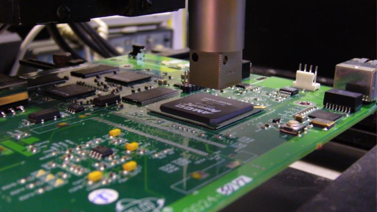
10 Tips for PCB Stackup Design
With the continuous emergence of high-speed circuits, the complexity of PCB boards is also increasing. In order to avoid the interference of electrical factors, the signal plane and the power supply layer must be separated, so it involves the design of a multi-layer PCB, that is, the design of the laminated structure.
1. Avoid direct connection of two signal planes
A multi-layer PCB, usually includes a signal layer (S), a power layer (P) layer, and a ground layer (GND). How are the three arranged?
Power and ground planes are usually inseparable solid layers that provide a good low-impedance current return path for current from adjacent signal traces. Therefore, the signal layer is mostly adjacent to the power layer or the ground layer. Moreover, the power supply layer and the ground plane use a large area of copper (so the power supply layer and the ground plane are also called copper layers). The large copper film can provide shielding for the signal plane, which is conducive to impedance control and improvement of signal quality.
Also, try to avoid two signal planes that are directly adjacent to each other. Crosstalk can easily be introduced between adjacent signal planes, leading to circuit failure. Crosstalk can be effectively avoided by adding a ground plane between the two signal planes.
2. Most of the top and bottom planes are signal planes
The top and bottom surfaces of multilayer PCBs are typically used for components and a small number of traces, so they are mostly signal surfaces. Generally, the top layer is a component, and the bottom layer (the second layer) of the component can be set as the ground layer to provide the device shielding layer and provide a reference plane for the top layer wiring.
Also, note that these signal traces on the top and bottom planes cannot be too long to reduce direct radiation from the traces.
3. Reference planes prefer ground planes
Both the power supply layer and the ground layer can be used as reference layers and have a certain shielding effect.
The difference between the two is that the characteristic impedance of the power supply layer is high, and there is a large potential difference with the reference level; while the ground plane is generally grounded. As the reference point of the reference level, its shielding effect is much better than that of the power supply layer.
Therefore, when choosing a reference plane, strata are preferred.
4. The high-speed signal layer is located in the middle plane of the signal
The high-speed signal transmission layer in the circuit should be a signal intermediate layer, sandwiched between two copper layers. In this way, the copper film of the two copper layers can provide electromagnetic shielding for high-speed signal transmission, and at the same time can effectively limit the radiation of high-speed signals between the two copper layers without causing external interference.
5. The power layer and the ground layer are best paired
The power supply layer and the ground plane appear in pairs. Shortening the distance between the power supply and the ground plane can reduce the impedance of the power supply, which is beneficial to the stability of the power supply and reduces EMI. In particular, the mains should be as close as possible to their corresponding ground planes. In the case of high speed, additional ground planes can be added to isolate the signal plane, but it is not recommended to add more power planes for isolation, because the power plane will bring more high-frequency noise interference.
6. Copper layer balance design
The copper layers, i.e. the power layer or the ground layer, should preferably be arranged symmetrically, such as the second and fifth layers of a 6-layer board, or the third and fourth layers should be copper plated together, which is considered flat and level in the process of. Construction requirements, as unbalanced copper layers can cause warpage as the PCB expands.
7. Multiple power planes away from high-speed signal planes
Multiple power planes should be kept away from high-speed digital signal routing. Because the multi-power supply layer is divided into several physical regions with different voltages, if the signal power supply is close to the multi-power supply layer, the signal current on the nearby signal layer will encounter an unsatisfactory return path, causing a gap in the return path.
8. Use even layers
The classic PCB stack-up design is almost entirely even, not odd. Even-numbered layers of a printed circuit board have cost advantages, and even-numbered layers are more resistant to board warpage than odd-numbered layers.
9. Arrange routing on adjacent layers
In order to complete complex wiring, the transition of traces between layers is inevitable. The two layers that the signal path spans are called "routing combinations". The best layout combination design is to avoid the flow of backflow current from one reference plane to another reference plane but to flow from one point (surface) of one reference plane to another point (surface).
Therefore, wiring combinations are preferably arranged on adjacent layers, since the path through the layers is not clear for return currents. Although ground bounce can be reduced by placing decoupling capacitors near the vias or reducing the thickness of the dielectric between the reference planes, this is not a good design.
10. The trace directions of adjacent signal planes are orthogonal
On the same signal plane, the directions of most of the traces should be the same and should be orthogonal to the trace directions of the adjacent signal planes. For example, the wiring direction of one signal plane may be the "Y-axis" direction, and the wiring direction of the other adjacent signal plane may be the "X-axis" direction.
The above describes 10 tips for PCB stack-up design. If you want to customize or buy PCB boards or want to assemble PCB boards, please contact us.
Singo is a professional custom PCB board manufacturer. We provide full-service PCB assembly and fabrication, so you can have our team throughout the conceptualization phase and successful product launch. Our priority is to provide a high standard of work and fast turnaround times in everything we do for you. We have advanced equipment and skilled engineers to provide a variety of electronic manufacturing services and can complete short-term production of up to 10,000 units at a time.
