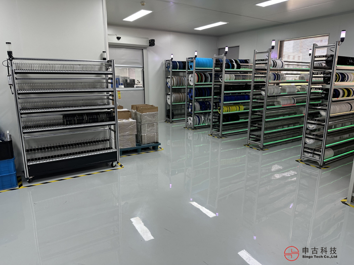
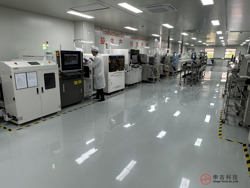
At singo, all materials must be verified and approved before entering the warehouse. Singo has established strict verification procedures and work instructions to control incoming materials. In addition, Singo has a variety of sophisticated testing equipment to ensure that it can correctly judge the quality of the material to be verified. Singo uses a computer system to manage materials to ensure that materials are first in, first out. When a material is close to the expiration date, the system will issue a warning to ensure that the material is used up before expiration or is verified before use.

Quality Policy
One
Home / Quality Policy
- Raw material inspection
- PCBA function test
- AOI
- First Article Inspection
- X-Ray Inspection
- Visual Inspection + Random Inspection
1. Incoming Quality Control (raw material inspection)
Incoming Quality Control (raw material inspection)
To make sure the components to be used are good quality, there are several processes that we follow:
1)An overview of the visual electronic components inspection process includes:
* Packaging examined:
-Weighed and checked for damage
-Taping condition inspected-dented package etc.
-Original factory sealed vs. non-factory sealed
* Shipping documents verified
-Country of origin
-Purchase order and sales order numbers match
* Manufacturer P/N, quantity, date code verification, RoHS
* Moisture barrier protection verified (MSL)-vacuum sealed and humidity indicator with specification (HIC)
* Products and packaging (photographed and cataloged)
* Body marking inspection (faded markings, broken text, double print, ink stamps, etc.)
* Physical conditions inspection (lead bands, scratches, chipped edges, etc.)
* Any other visual irregularities found
2) Engineering Components Inspection
Our highly skilled and trained engineers receive the components for evaluation at a microscopic level to ensure consistency and quality. Any suspect parts or discrepancies that are discovered in the visual inspection process will either be verified or discounted by taking a product sampling of the material/parts.
* Review visual inspection findings and notes
* Purchase and sales orders numbers verified
* Verification of labels (bar codes)
* Manufacturer’s logo and date log verification
* Moisture sensitivity level (MSL) and RoHS status
* Extensive marking permanency tests
* Review and comparison to manufacturer datasheet
* Additional photos taken and cataloged
* Solderibility Testing, the samples undergo an accelerated ‘aging ‘ process before being tested for solderibility, to take into
consideration the natural aging effects of storage prior to board- mounting; In addition to the Engineering Components Inspection we have a higher level of inspection under the customer request.
3) By customer request, all components can pass a thorough final inspection in our Assembly facility.
Quality Policy
* We will strive for total customer satisfaction by continuous improvement for the Quality and the Processes of all our business activities to deliver high quality of product and premium value products on time
* Quality Objectives
* 1.Continuous Improvement
* High quality of product
* Improvement Projects
One
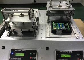
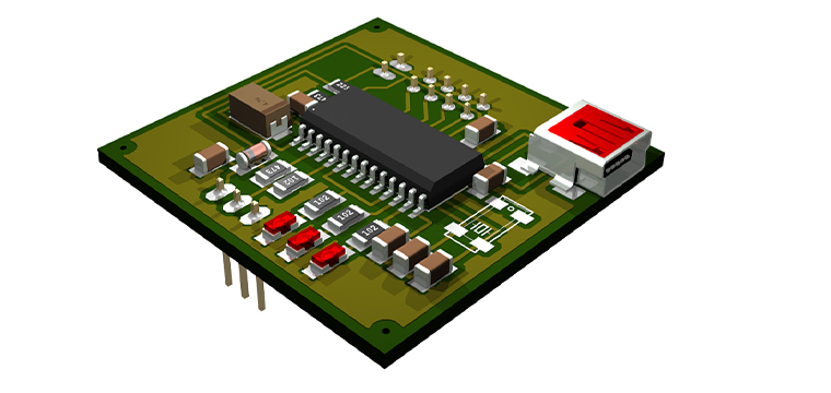
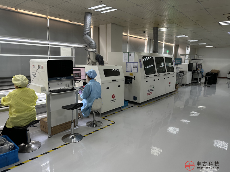
2. PCBA Test – The Key to Guarantee PCB functional by SMT Test (PCBA function test)
Inspection and testing are essential aspects of bringing a product to market. A persistent failure or recall issue can not only cost you money, but can also do irreparable damage to your reputation for quality. For this reason alone, it’s essential to partner with a PCB manufacturer who offers comprehensive circuit board testing.
PCBA SMT assembly processing could be very complicated, which include PCB board production process, component procurement and inspection, SMT assembly, DIP, assembly and PCBA test. Among them, PCBA test is the most important control step inside the whole PCBA processing. The test determines the very last performance of the product.
2.1 So what are the PCBA test?
1) The ICT test mainly includes circuit continuity, voltage,current values, fluctuation curves, amplitude, and noise.
2) FCT testing requires IC programburning, simulation testing of the entire PCBA board function, discovery of hardware and software problems, and equipped with necessary SMT processing production fixtures and test racks.
3) Aging test is mainly to energize the PCBA board and electronic products for an extended period. The test continuously keeps the product in operation and observe any failures. After the aging test, the electronic products can be sold in batches.
4) The fatigue test mainly takes samples of the PCBA board and performs high-frequency and long-term operation to observe whether there are failures and determine the probability of failure in the test. This is to provide feedback on the operational performance of the PCBA board in the electronic product.
5) The test in harsh environments mainly exposes-the PCBA board to extreme temperature, humidity, drop, splashing, and vibration. It obtains the test results of random samples to infer the reliability of the entire PCBA board batch product.
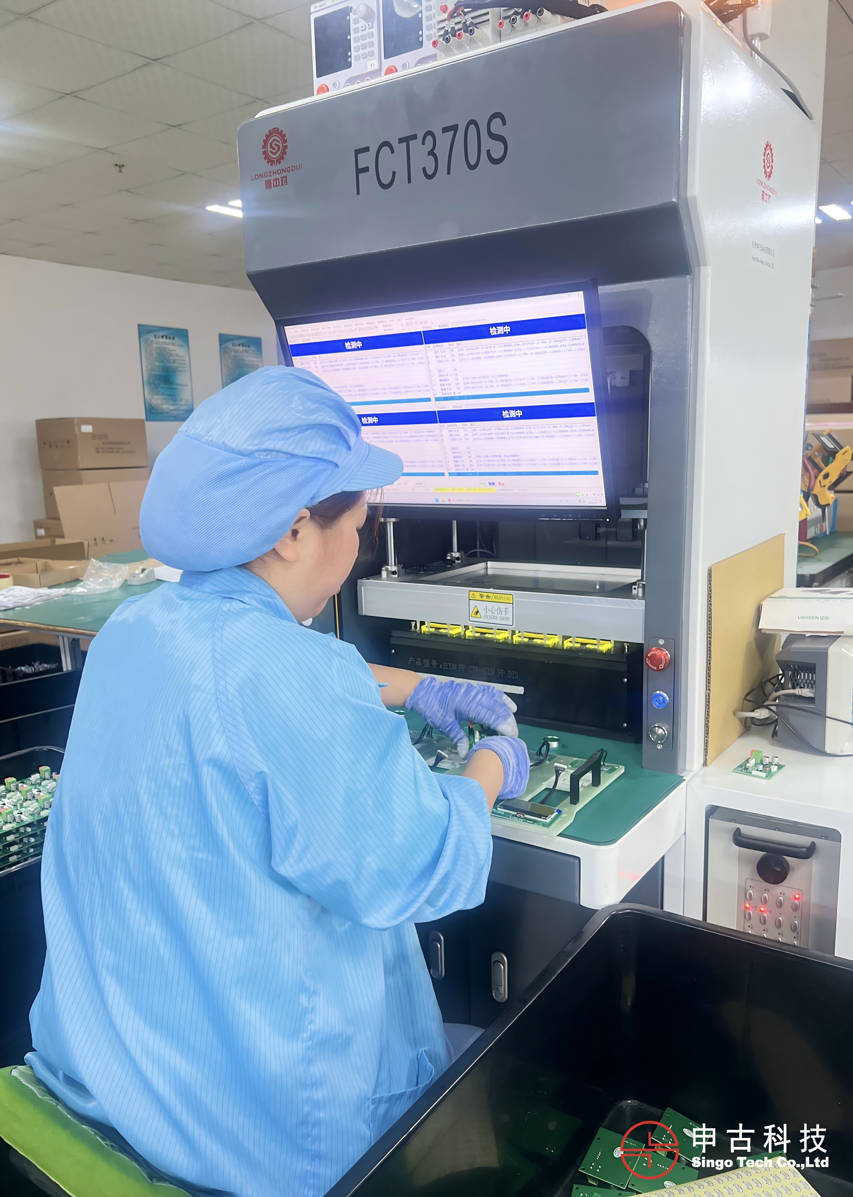
The PCBA process is complicated. Various problems may occur during the production and processing due to improper equipment or operation, and there is no guarantee that the products produced are qualified. Therefore, PCB testing is required to ensure that each product does not have quality problems.
We conducted tests using professional FCT equipment to ensure that each PCBA met the requirements.
One
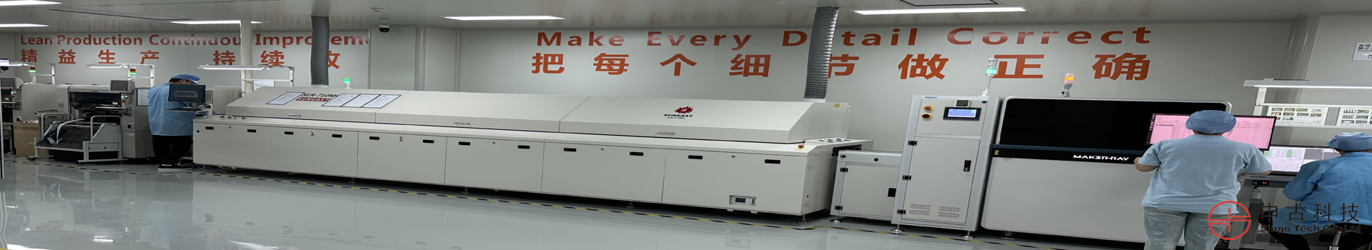
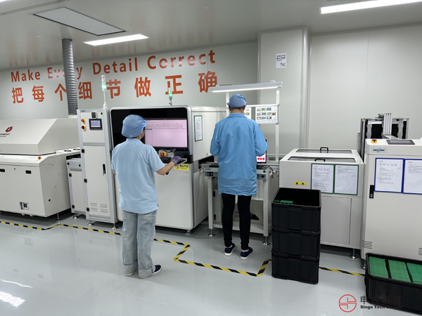
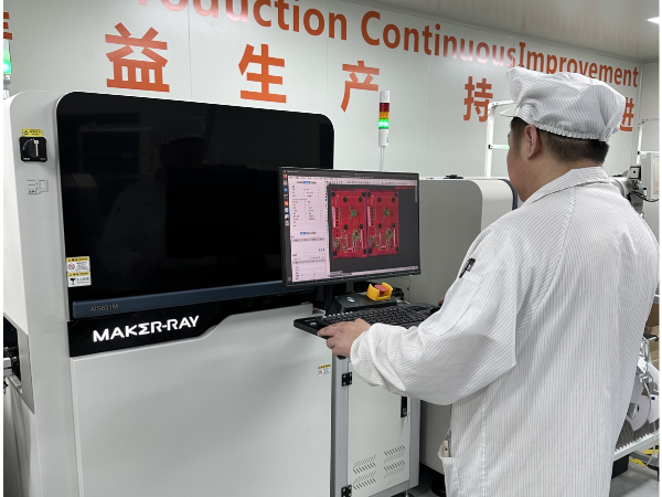
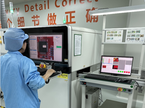
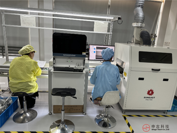
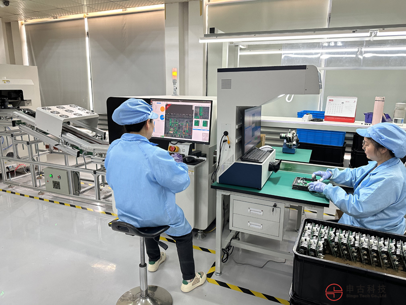
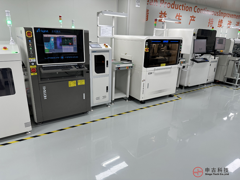
3.Automated Optical Inspection (AOI)
The modern PCB features almost countless joints, thus making the manual inspection a challenging task. Keep in mind that even in the years of simpler PCB circuit boards, manual testing was still hard and resulted in imperfect outcomes.
Think of the human factor. Human inspectors get tired, lose attention, or accidentally overlook some defects. It’s clear that with more advancement in these products, manual testing can’t keep pace with the exacting demands required. Moreover, vast quantities of PCBs are needed to satisfy the large and growing demand for electronic circuits. So, one needs more rapid and accurate methods. For all this, the only answer is an automatic optical inspection system. PCBA SMT assembly processing could be very complicated, which include PCB board production process, component procurement and inspection, SMT assembly, DIP, assembly and PCBA test. Among them, PCBA test is the most important control step inside the whole PCBA processing. The test determines the very last performance of the product.
3D SPI
Detects of solder paste height, area, volume; excessive solder, insufficient solder, solder peaks, solder bridges, XY offset, angular offset, etc.To ensure flawless solder paste printing on every PCBA.
3D AOI
Detects of SMT components(wrong part, missing part, reversed part, extra part, flipped part, XY offset, angular offset, damaged component, lifting, tombstoning, side-standing, raised lead, poor solder joint, bent lead); and wetting (height, volume, area), excessive solder, insufficient solder, solder bridges, poor solder joint, voids, solder balls, insufficient lead protrusion, bent leads with insufficient protrusion, etc.)
To ensure correct component placement and optimal soldering quality on every PCBA.
AOI in front of DIP furnace
Detects of wrong part, missing part, reversed part, extra part, misalignment.
To ensure the correctness of every through-hole (DIP) component on the PCBA before wave soldering.

AOI behind of DIP furnace
Detects of excessive solder, insufficient solder, solder bridges, insufficient lead protrusion, bent leads with insufficient protrusion, poor solder joints, voids, solder balls, etc.
To ensure excellent and flawless soldering of every through-hole (DIP) component on the PCBA.
3.1 How does AOI PCB accomplish its stunning results? Here we list three basic approaches
1) Template matching – this method compares the image captured with that of the “golden board,” which acts as a benchmark. So anything that is a mismatch to this board is flagged
2) Pattern matching – the system keeps a store of the image of the ideal PCB board and to match the actual output with the stored image in order to identify flawed products
3) Statistical pattern matching – This technique resembles pattern matching but uses large numbers of board images. Following this, It then applies methods of statistics to identify flaws. Consequently, this method will also not reject all board errors, as some are too minor to need flagging.
We do a 3D automated optical inspection of PCBs at a very early stage of the production run. After the soldering stage is done, we deploy the technique. The value of this is that we can detect flaws early enough and correct them. Since these defects are detected early rather than later in the production process, the savings in cost and time are great.Also, the automated optical inspection system benefits from a feedback process. When defects emerge, they are promptly detected and relayed back to earlier stages. Therefore, we are able to catch and remove flaws so that not too many boards with the same defects appearFor Bare printed circuit boards, The AOI test verifies the finished conductor trace image for deviations from the Gerber data and finds errors that the E-Test may not discover, such as (for example) narrowed, but still unbroken conductor traces.
3.2 The AOI test is especially important for the following application areas:
(1) High frequency
(2) High power loads
(3) High data transmission rates
(4) Op-amps with high amplification factors and input resistances The inner layers of multilayer PCB use AOI to scan before they are pressed together. This guarantees the high reliability of multilayer boards.
(2) High power loads
(3) High data transmission rates
(4) Op-amps with high amplification factors and input resistances The inner layers of multilayer PCB use AOI to scan before they are pressed together. This guarantees the high reliability of multilayer boards.
3.3 How is AOI Working
- (1) The AOI inspection is done by scanning the surface of the PCB board.
The AOI machine fitted with HD color cameras that scans the surface with high magnification clearly showing on larger monitor screen the details of each section of PCB and each component of each section. The camera captures the image of the PCB surface through light source such as fluorescent or LED lights pcb or UV or infra red light.
The image is then compared with the pre-programmed data and fed in the memory of AOI processing system. The difference or Normalized Cross Correlation (NCC) if found greater than tolerance limit is displayed and indicated and process is stopped immediately. The higher the NCC the smaller the difference in captured and pre-programmed (template) images. The final decision to declare the board to be faulty and hence stop process depends on various algorithms running on AOI machine depending on pixel counts and NCC values.
- (2) Operator of AOI machine
The operator of AOI machine also visually checks the images captured by AOI machine on screen and hence can manually stop process as found necessary. The blob analysis is performed by separating the object image from background and then integrating or grouping the “blobs or pixels” of pixels based image and finding faults.
- (3) The AOI can be done before reflow to check for component placement,
The AOI can be done before reflow to check for component placement, location and status i.e. defects not related to soldering. The post reflow AOI identifies defects in soldering joints, components and PCB board itself that may have caused due to thermal dynamics of reflow oven
- (4) The AOI machine can scan smallest components such as 0105,
The AOI machine can scan smallest components such as 0105, 0201 and 0402 package and IC packages like QFP, QFN, CSP and BGA and PoP only for surface inspection not for underneath the package inspection. It should be noted that components that are present under the body/package of IC cannot be inspected by AOI.
For this AXI is required. Because X-Ray can penetrate through the body then the grey scale images can be shown for the component identification beneath the IC package.
3.4 Types of Faults AOI can Inspect:
The AOI is an impressive method of automated inspection of PCBs on mass scale production line. The AOI can check for open and short circuits, wrong polarity of components, misplaced or missing components, wrong orientation of IC packages, stains, cuts, scratches, insufficient solder paste, solder bridges, cracked solder joints, excess solder, lifted leads, tombstoning, solder balls, billboarding, package height (3D AOI), coplanarity (3D AOI)
Types of Faults AOI cannot Detect:
Wrong values of components, counterfeit component, BGA package shorts and opens, solder quality,
3.5 Why AOI preferred over Visual Inspection:
here are many reason as to why one should opt for AOI inspection rather than visual. But visual inspection is still incorporated in many PCB fabrication house. Some of the main reasons to select AOI over visual inspection are
1- Human eye can get tired and fatigue is common while doing visual inspection of tiny components on PCB. On the other hand machines do not get tired not fatigue
2- Human visual inspection is susceptible errors and can mistakenly miss the fault on PCB. While AOI machine will never miss a fault if that fault details are programmed in AOI machine memory. Hence accuracy of AOI is better than visual inspection
3- Humans can get sick of doing same type of job while machines can do the same job repeatedly, precisely forever.
4- AOI is helpful for mass production runs of PCB fabrication and assembly while visual inspection is not suitable for mass production and suitable for prototype level production
5- AOI is faster and can save time and money while visual inspection is slow and needs more focus and time to complete inspection
6- AOI is machine based inspection method hence it gives valuable data logging of types of errors or defect that occur in various stages of PCB fabrication and PCBA. While visual inspection many times do not record the faults and types of defect but can rectify the defects easily.
7- With AOI you will be assured that your PCB will be completely defect free and with visual inspection there are always chances that some defects are remaining
Conclusion:
Summing up all we can say that AOI is utmost important aspect of PCB fabrication and PCB assembly processes. It is flexible to be implemented at any stage of process as per the requirements of user or needs. For mass production of complicated SMT based PCBs it is highly recommended to run AOI.
One
4. First Article Inspection-First Article Inspection in the PCB Assembly Process
First Article Inspection-First Article Inspection in the PCB Assembly Processcontact us
Singo tech offers first article sampling services, to ensure our customers are satisfied with our quality of work before proceeding to full production. This service would not be possible without first article inspection (FAI), which involves the inspection and testing of the very first PCB to go through each stage of the assembly process. This master circuit board is given special priority, as it is the standard which we use to ensure our assembly equipment has been calibrated, programmed, and is functioning correctly. First article inspection incorporates the parts management, 3D solder paste inspection (SPI), automated optical inspection (AOI), 3D AOI, instrumentation, parts orientation and reference verification processes.
Our qualified assembly technicians will verify that all components for each order match the customer’s design and BOM. Once this is done, after each step of the assembly stage, our quality engineer will inspect the circuit board visually, through automated SPI and AOI machines for any issues in solder paste application and component placement. This will ensure that any possible maladjustments are caught and rectified immediately, before starting the complete assembly run.
Our quality engineer will then conduct measurements with our state-of-the-art FAI system, to ensure that every part has been placed correctly, before finally soldering them onto the printed circuit board. The FAI system generates a report, which our engineer and technicians use to determine if the PCB was assembled correctly, or if further adjustment to our manufacturing equipment is necessary. And once the board has been finally soldered, it will be subjected to visual inspection, X-ray inspection (for BGA components) and functional circuit test. If any issues arise during assembly, our FAI process will allow us to adjust our manufacturing equipment accordingly. After passing all quality checks, we will provide high resolution images of the board to our customers for approval, before completing the order.
Our first article sampling service grants customers the opportunity to assess the quality level of their PCBs, before proceeding to full production. Through this service, customers will receive a small sample of PCBAs for approval before the rest of the order is assembled. The exact number of samples can be determined with your sales representative during the quoting process. At Singo, we will go the extra mile to make sure your orders are fulfilled to your satisfaction, with only the best results.
One
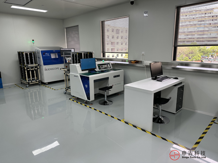
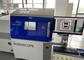
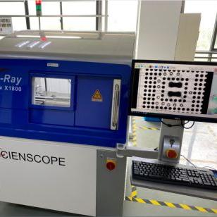
5. X-Ray Inspection for BGA Assembly (X-Ray Inspection)
X-Ray Inspection for BGA Assembly (X-Ray Inspection)
Our automated X-ray inspection systems are able to monitor a variety of aspects of a printed circuit board in assembly production. The inspection is done after the soldering process to monitor defects in soldering quality. Our equipment is able to”see” solder joints that are under packages such as BGAs, CSPs and FLIP chips WHERE the solder joints are hidden.
This allows us to verify that the assembly is done right. The defects and other information detected by the inspection system can be quickly analyzed and the process altered to reduce the defects and improve the quality of the final products. In this way not only are actual faults detected, but the process can be altered to reduce the fault levels on the boards coming through. Use of this equipment allows us to ensure that the highest standards are maintained in our assembly.
Singo invest 3D Automatic X-Ray Inspection machines to detect QFN,FBGA and other lead-less package types components, The X-ray images can help us also to analyse root causes of detective boards, such as excessive solder, lack of solder, mechanical failures of components, cracks, but also to detect hidden problems inside the PCB, such as bad metallisation in the holes or via cracks, This technique contributes greatly to Singo’s Quality Management strategy for complex components.
X-Ray inspection:X-ray inspection uses high power that generates from cathode rays to strike metal. X-ray appeared to lose kinetic energy from electronic slow down suddenly. The position that can’t be inspected will use an x-ray to inspect the change of light intensity. The image will show the inner structure to find out which area or position has the problem.With the rapid development of electronic technology, SMT technology is already universal. The chips’ footprint is smaller with more pins, especially when BGA came out in recent years. The BGA design is not like the conventional design with pins distributed all around, but distributed at the bottom of the chips. There is no doubt that it is difficult to determine whether the soldering work is good or not by traditional artificial visual examination.
That is why we must conduct ICT and functional tests. It is hard to fix if bad solder work is found at mass production. Artificial vision is a technology which the lowest precision and repeatable results. The X-ray test is widely used in SMT reflow soldering work inspection and can analyze qualitative and quantitative solder joints, and determine the fault and repair it in time.
5.1 X-ray inspection application :
IC, BGA, PCB/PCBA, SMT inspect, etc.
 IC
IC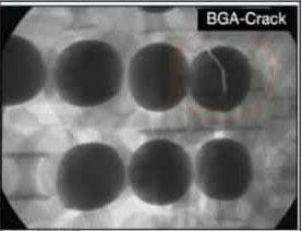 BGA
BGA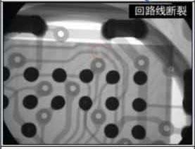 PCB/PCBA
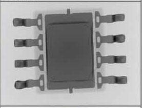 SMT inspect
5.2 Test steps
 1.Confirm the type of material of sample
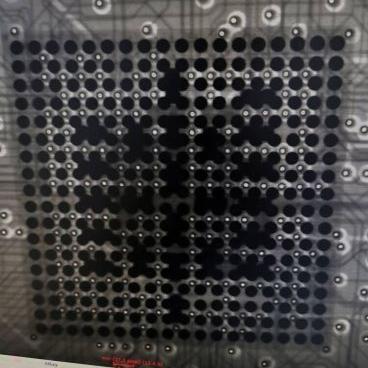 2.sample put on PCB x-ray machine
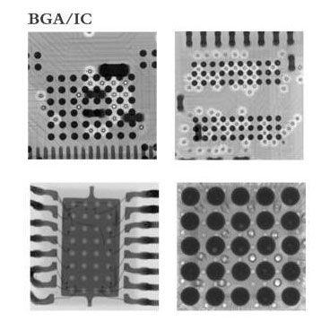 3.analyze the image
 4.marked the fault position and type
5.3 The advantages of using X-Ray inspection equipment as below
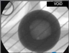
(1) The inspection effectiveness rate is about 97%, and such defects can be inspected: Cool solder, tin connect, not enough solder, components missing, etc. In particular, an X-Ray can also check BGA, CSP, and other hidden solder joint devices
(2) High test range, X-ray can test inside of the sample.
(3) Short inspection time.
(4) Find defects that cannot be reliably detected by other testing methods, such as cool solder, air holes, and poor forming.
(5) Only need to inspect 2-layer or multi-layer once.
(6) Provide measurement information to evaluate the production process, such as solder paste thickness, solder amount under the solder joint, etc.
What cause Cool solder:
The PCB board vias quality is poor. It will affect components parameter and make electrical conductivity of the multi-layer assembly. The inner line is unstable, resulting in the failure of the entire circuit function.Circuit boards and parts warp during welding, and soldering and short circuit can occur due to stress and deformation. Warping is usually caused by a temperature imbalance between the top and bottom of a circuit board.
The PCB design will affect PCB solder quality.
The reason for adhesion: The temperature of the iron should not be too high. The high temperature will make the iron head burn and can not get tin, and easy to fall off the copper foil. The copper foil falls off because the soldering iron should not get too much tin at one time, as too much tin will cause adhesion between the two solder joints.
X-ray can inspect the PCB defects such as cool soldering, adhesion, copper foil falling off.
IC X-ray inspection device mainly uses X-ray to illuminate internal chips. The intense penetration of X-ray can penetrate the chip then create an image. The image will show the chip internal structure fracture situation in a complete view. The main feature of the X-ray is to make sure the chip does not have damage to the chip itself, so this detection method is also called nondestructive flaw detection.The IC X-ray inspection machine adopts the principle of X-ray transmission to take pictures of the measured object’s internal structure in real-time. Widely used in battery, electronic products processing, casting processing, and other industries, the main product internal defects can be used for practical analysis. Users can easily obtain high-quality, high-magnification, and high-resolution images.
With the development of communication, computer, consumer electronics, and other industries, the future development trend is a smaller ICT space, more invisible welding joints such as BGA, and higher requirements for welding quality. As an emerging process method and analysis,
X-ray detection technology can detect invisible defects under the premise of not destroying the product, reflecting the product’s internal information, and carrying out qualitative and quantitative analysis on the detection results. This is an advantage to find the fault as early as possible and reduce the rejection rate. Our X-Ray machine has been widely used in PCB surface mount to ensure that we can provide customers with high-quality PCBA products.
One
6. Visual inspection + random inspection
In the last step of the process a team of sharp-eyed inspectors give each PCB a final careful check-over.Visual checking the PCB against acceptance criteria and using singo “approved” inspectors. Using manual visual inspection and AVI – compares PCB to gerber and has a faster checking speed that human eyes, but still requires human verification. All orders are also subjected to a full inspection including dimensional, solderability, etc.contact us

Singo is a full-service PCB assembly company, so you have our team available throughout the conceptualization stage and to a successful product launch. Our priority is delivering a high standard of work with quick turnaround times in everything we do for you. Our advanced equipment and skilled engineers perform a multitude of electronic manufacturing services, completing short-run productions of up to 10,000 units at a time.