
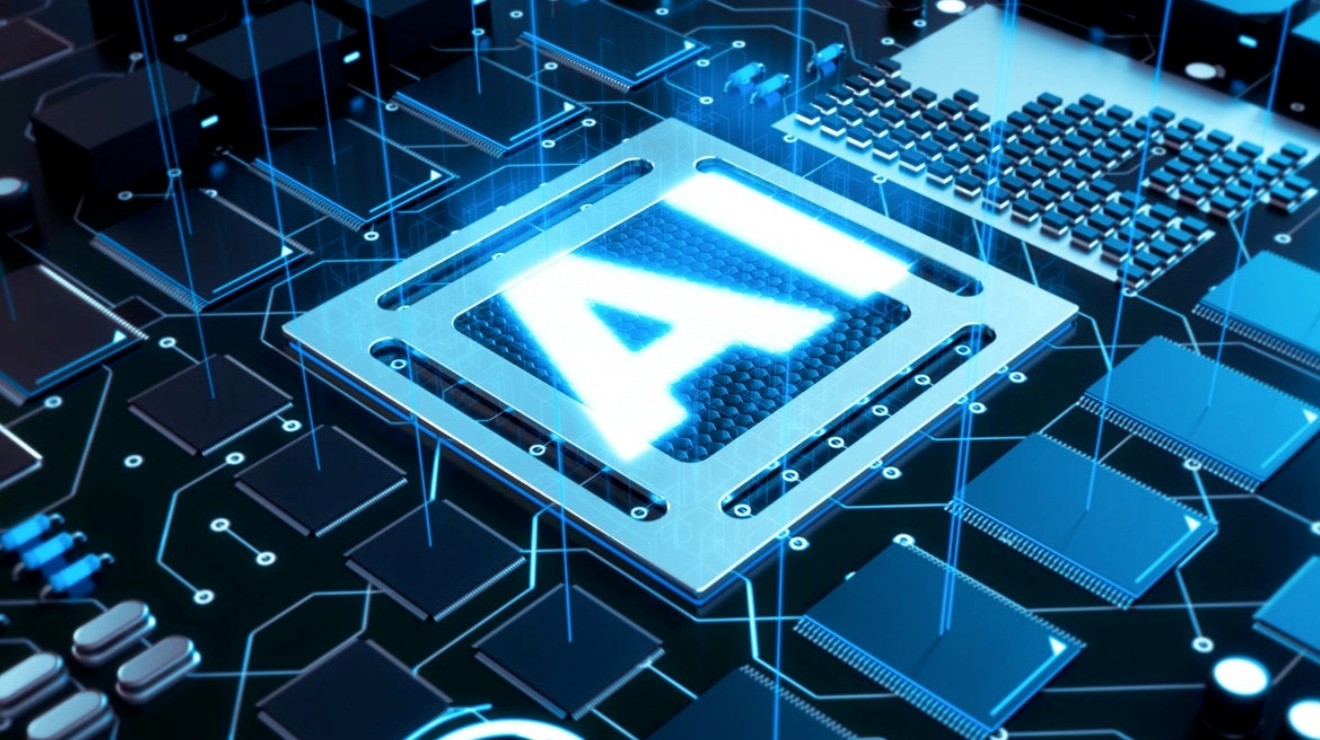
The Future of PCBs is Here: The Impact of AI on the Electronics Industry
Artificial intelligence, or AI, has been invading our technological world for the past decade. Artificial intelligence is a forward-looking and futuristic concept that is being widely used in various applications in almost all industries. As a result, we now have Alexa, Siri, and many other AI-powered voice assistants, self-driving cars, internet search engines, and more. The use of artificial intelligence is spreading widely and growing exponentially.
According to Singo, PCBs, or printed circuit boards, affect AI applications in two main ways, and vice versa:
PCB for Devices Using AI
The trend in the electronics industry is to make devices smarter. Embedding artificial intelligence in robots, voice assistants and self-driving cars can help achieve this by using advanced microcontrollers and other electronic components. All electronic devices require printed circuit boards to function, and devices using AI are no exception. However, the introduction of artificial intelligence into devices is a futuristic concept, and this process brings new challenges to PCB design and manufacturing.
Artificial Intelligence Impacts PCB Design and Manufacturing
Just as smart devices using AI need PCBs to function, PCB designers and manufacturers are leveraging AI. AI is helping them develop newer, more efficient methods of PCB manufacturing, optimize costs, reduce scrap and turnaround time, and improve supply chain, inventory, and asset utilization.
AI helps in two ways - it helps systems communicate with each other, and it helps systems communicate with operators. For example, during PCB assembly, AI helps determine the precise placement of SMD components. This not only reduces assembly time, but also significantly improves the quality of the board. With the electronics industry's rapid trend toward miniaturized form factors, quick and accurate component placement prior to soldering is a huge advantage.
Using Printed Circuit Boards for AI Applications
All electronic devices, whether using artificial intelligence or not, require printed circuit boards to function. Implementing AI in devices requires the additional incorporation of specialized tiny components, typically SoCs, flip-chips, and tiny BGAs using fine-pitch packaging.
PCB manufacturers do this by creating circuit boards using a special technology called HDI, or High-Density Interconnect. HDI allows very high component densities through the use of thin, closely spaced traces and very small vias or micro vias.
Advantages of HDI Technology
HDI technology is a major contributor to the improvement in PCB performance required for devices in AI applications. HDI not only makes PCBs smaller, lighter, and thinner but also improves electrical performance. Some advantages of using HDI technology are:
- Very low electrical parasitics - low EMI, high-speed operation, better signal integrity
- Minimal stub - low signal reflection
- Stable voltage - low track resistance
- No need for decoupling capacitors - due to low electrical parasitics
- Lower noise and crosstalk - due to better signal integrity
- Low EMI and RFI - due to micro vias, vias in pads, and surface ground planes
- Closer ground plane
- Better distributed capacitance
The advantages of using HDI technology are further supported by semiconductor manufacturers offering smaller components. The overall size of the board and components is smaller, and the rise and fall times of the signals are faster. This manifests itself in better high-frequency operation.
However, smaller component sizes mean less surface area for heat dissipation. Therefore, HDI needs better thermal management. PCB manufacturers achieve this by using high-performance laminates. In addition to better thermal management, high-performance laminates help improve signal integrity. The use of stacked microwells also helps improve the high-speed performance of HDI boards.
Laser-drilled micro vias are almost one-tenth the size of mechanically drilled holes. Thus, micro vias have the advantage of lower parasitics and inductance while improving high-speed performance.
Artificial intelligence offers significant advantages in the circuit board inspection process. AI logic is very effective for finding defects such as wrong components, missing components, misplaced components, and tracking defects. This is especially useful when using tightly packed tiny components on HDI boards.
AI Enhancements for PCBs
PCBs serve as platforms for the interaction of miniature electronic components and systems, and their design and manufacturing processes have a significant impact on electronic devices. Hence, PCB manufacturers rely on AI-induced board design and quality enhancements.
When designing a new PCB for an application, designers take care to make the best possible use of the available space while packing components as close together as possible to avoid failure. The current design process relies heavily on the experience of engineers, and the design must be verified by actual experiments. Documentation of test results is easily overlooked in most cases, leading to repeated testing of error-prone designs, further increasing costs.
Quality Assurance Requires High Investment
The complex design of PCBs requires the manufacturing process to follow strict specifications. To achieve this goal, each PCB undergoes rigorous testing upon completion. Typically, one of these tests is an automated optical inspection or AOI.
AOI uses image analysis techniques to determine whether manufactured PCBs meet design specifications and are free of technical defects. However, the methods currently used produce a high rate of false negatives, misclassifying many boards as defective.
These misclassified boards then require another level of human or machine inspection. As a result, high false negative rates can falsely reject non-defective PCBs, which then require re-inspection, increasing costs. On the other hand, a low false positive rate can mean high follow-up costs as many defective boards enter the workflow. All of this means that it is difficult to achieve the desired positive or false negative rates with existing AOI and manual inspection methods.
Best Choice Self-Study Tips
FIT demonstrates what AI can do in the inspection process of the future. The process is the same as traditional AOI, i.e. a camera captures an image of the PCB. In this case, however, high-quality images are crucial because these images will be the training data for the AI modules. Only selected images must reach the modules of machine learning and deep learning.
The modular design has a variety of algorithms, which can continuously improve its own performance. Continuous automated inspection of the board continuously feeds the resulting data back into the algorithm. This forms the self-learning process of the AI module. Feedback enhances the database while optimizing the true-negative rate. Real industrial experience with this module shows a 20% reduction in the use of production resources.
Intelligent PCB Design and Manufacturing
After completing the training, the AI module can also help design new PCBs. This helps reduce the time it takes to place components on a board using the trial and error method that designers today use to arrive at the best configuration. Instead, AI module algorithms help predict the best configuration for optimal functionality.
PCB design is just one example of how self-augmenting AI modules can help enhance quality assurance. This self-learning AI module is equally effective in other areas of the PCB manufacturing process, such as optimizing the etch process, reflow process, and other time-intensive activities, resulting in significant time and production cost savings.
Deep Learning and Machine Learning
Many industries, including PCB manufacturing, are benefiting from deep learning and machine learning through artificial intelligence. Essentially, it requires the efficient use of data to gain experience in solving complex problems with little to no human intervention. Machine learning and deep learning, when applied to the PCB design and manufacturing process, can not only greatly improve operations, but also reduce the cost of human intervention.
In Conclusion
According to Singo, the positive impact of AI in PCB manufacturing is priceless. However, the industry must carefully develop the aforementioned factors to fully exploit the enormous potential of AI. This requires dedicating sufficient time and resources to use artificial intelligence in the PCB manufacturing process. Ultimately, this could usher in an era in which production processes are completely streamlined and outcomes improve exponentially.
Singo is a professional custom PCB board manufacturer, mainly engaged in PCB assembly and OEM/ODM electronic manufacturing services since 2006. Products related to medical equipment, home appliances, digital products, industrial control, etc. After years of hard work, we have established long-term cooperative relationships with some internationally renowned companies. If you are looking for electronic PCBA OEM/ODM suppliers, welcome to contact us, we sincerely welcome you to visit our company.
