
PCB Vias: Understanding Microvia Design
Printed circuit boards are at the heart of electronics as they provide the conductive pathways through which all electronic components connect and work together. As electronics become more advanced and complex, PCBs sandwich multiple layers together to make all the necessary connections.
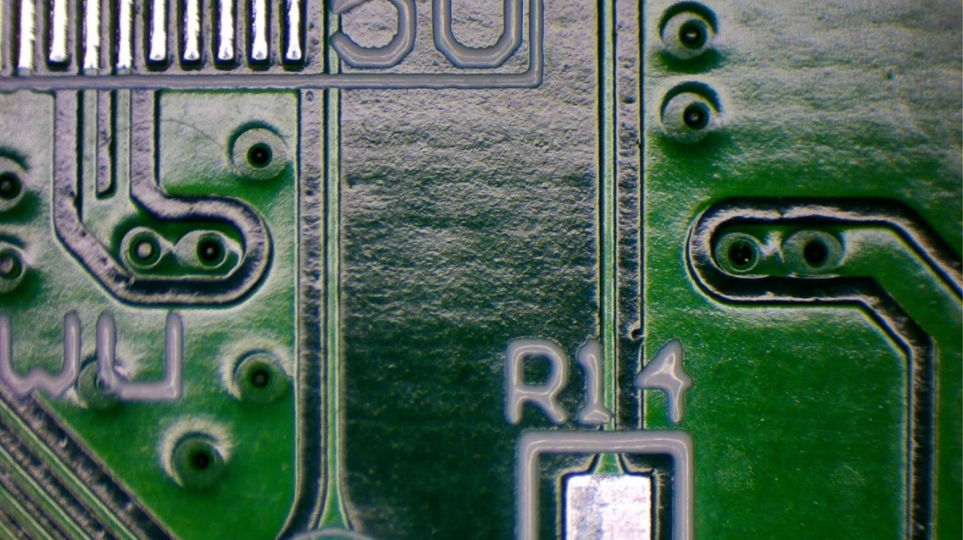
To make electrical connections between layers, holes need to be drilled throughout the PCB, connecting all the layers together when the holes are copper plated. These are called plated through holes or vias. Depending on the diameter, pores can be considered micropores.
What are Micropores?
According to the Printed Circuit Board Association, a micro via is any hole drilled in a PCB with a 1:1 aspect ratio but no deeper than 0.010 inches. Previously, IPC considered micro vias based on their size if they were 0.006 inches or smaller. However, changing technology now allows lasers to frequently drill such tiny holes.
IPC decided to adopt a new microwell definition with a 1:1 aspect ratio and a depth threshold of 0.010 inches to prevent constant changes to its definition. Microvias, also known as uveas, can be used to connect layers within a PCB. However, they usually do not connect more than two layers in a row.
Different Types of Micropores
There are many types of micro vias that PCB designers can drill. Each type of microwell has the same size aspect ratio. The main difference between them is their location.
Blind Microvias - Holes drilled to allow connection from a surface to another inner layer. These holes do not go all the way through the PCB like through holes but come from one side.
Buried Microvias - Holes in the inner layers of a PCB that do not reach any outer surface of the board.
Stacked Vias - Multiple blind and/or buried vias stacked on top of each other, allowing connections to inner layers.
Staggered Microvias - are layers of multiple buried micro vias connected. These microwells are not stacked on top of each other. Instead, they are placed offset from each other.
Via-In-Pad - involves placing a micro via directly on the copper pad of a component. This technique allows PCB miniaturization.
Advantages of Microvias for PCB Designers
PCB designers may find many benefits in using micro vias in their board designs. Microvias provide thermomechanical reliability to board functionality and performance. As circuit boards become smaller and lighter to fit mobile devices, the ability to create micro vias in pads allows for board miniaturization. Microvias save space on circuit boards due to their smaller size than normal through holes or plated through holes. By saving space, you don't have to have a larger circuit board to house all the necessary components that will be connected.
PCB designers can also minimize the risk of defects through micro vias because laser drilling is used. There are fewer manufacturing issues due to the shorter trace lengths. If creating HDI boards, micro vias can have a significant impact on signal integrity. When creating larger vias, more radiation is created for high-speed circuits. RF functionality is enhanced along with EMC properties when placed in microwells. Microvias are more reliable than other types of vias and vias.
When Designing Microvias on a PCB
There are several aspects to drilling micro vias for PCBs. When designing your board, keep in mind that the aspect ratio of micro vias should not exceed 1:1 when you are looking for holes that can be reliably plated. While it does drill holes at larger ratios, it's not reliable at all as it can cause plating defects. Also, our PCB designers never reduce the diameter below 4 mils, regardless of the aspect ratio. When first drilling into the copper surface with a laser drill, there should be no more than 1/2 oz of copper in the PCB design. As thicker copper is added, it makes it harder for the laser to drill and ablate to the next adjacent layer.
When placed in multiple layers, an additional lamination step is required for each layer that receives the vias. Holes that will not be used can be non-conductively filled or plated closed if desired. Since the micropores are so small, filling may not be required. Copper is used in electroplating, as a specialized bath, and chemicals are created for the process. Using this process, manufacturers gain greater flexibility in the design process.
If a layer is skipped, such as a blind micro via from layer 1 to layer 3, a gap is required through the layer along the second layer. However, if the second layer needs to be connected to the third layer, stacked or staggered micro vias can be used. However, staggered vias are easier to manufacture and provide higher reliability.
Summarize
Microvias provide PCB designers with manufacturing process flexibility as customers gain reliability when connecting multiple layers. When selecting materials for printed circuit boards, there are some materials that are better suited for the micro-via drilling process.
Talking to the PCB manufacturer before selecting a material group can give you an idea of the options available. Singo engineers have extensive experience in helping one select the right material for the application while being able to connect electrical components. In addition, you can use different micro-drilling processes to reduce material costs. By using vias, you can order smaller boards while saving space. You can potentially save a lot of money when you receive PCBs with minimal manufacturing defects and risks. If you want to order PCB boards, please contact us.
Singo is a professional custom PCB board manufacturer. The company is mainly engaged in PCB assembly and OEM/ODM electronic manufacturing services. Products include household appliances, digital products, industrial controls, medical equipment, etc. After years of hard work, we have established long-term cooperative relationships with some internationally renowned companies. Some of our products are frequently required to operate in harsh environments where quality and reliability are critical. With many years of experience, we have won a good reputation from customers in the field of electronic production with reasonable prices, abundant resources, and on-time delivery.
