Ten Golden Rules for PCB Design

Although the integration of semiconductors is getting higher and higher, many applications have a system-on-chip at any time, and many powerful, out-of-the-box development boards are becoming more and more readily available, many use-case applications in electronic products still require the use of Custom PCBs. In a one-off development, even an ordinary PCB can play a very important role. The PCB is the physical platform for design and the most flexible part of the original component electronic system design.
This article will describe ten golden rules that electronic design engineers should keep in mind and practice when using design software for PCB layout design and commercial manufacturing. Most of these rules have not changed since the birth of commercial PCB design 25 years ago, and are widely applicable to various PCB design projects.
Rule 1: Choose the Correct Grid Set and Always Use a Grid Spacing That Matches Most Components.
Although multi-grid seems to be effective, if engineers can think more in the early stage of PCB layout design, they can avoid the problems encountered in the interval setting and maximize the application value of the circuit board. Since many devices use multiple package sizes, engineers should use the product that is most beneficial to their design.
In addition, polygons are very important for circuit board copper. When multi-grid circuit boards are coated with polygonal copper, polygonal filling deviations will generally occur. While it's not as standard as being based on a single mesh, it can provide more board life than needed.
Rule 2: Keep Paths the Shortest and Most Direct.
This sounds simple and common, but it should be kept in mind at every stage, even if it means changing the board layout to optimize trace length.
Rule 3: Use Power Planes Whenever Possible to Manage the Distribution of Power and Ground Lines.
Power plane copper is a faster and easier option for most PCB design software. By connecting a large number of wires together, you can ensure that current is delivered with the highest efficiency and minimum impedance or voltage drop while providing an adequate return path to the ground.
Rule 4: Group Related Components Together with Required Test Points.
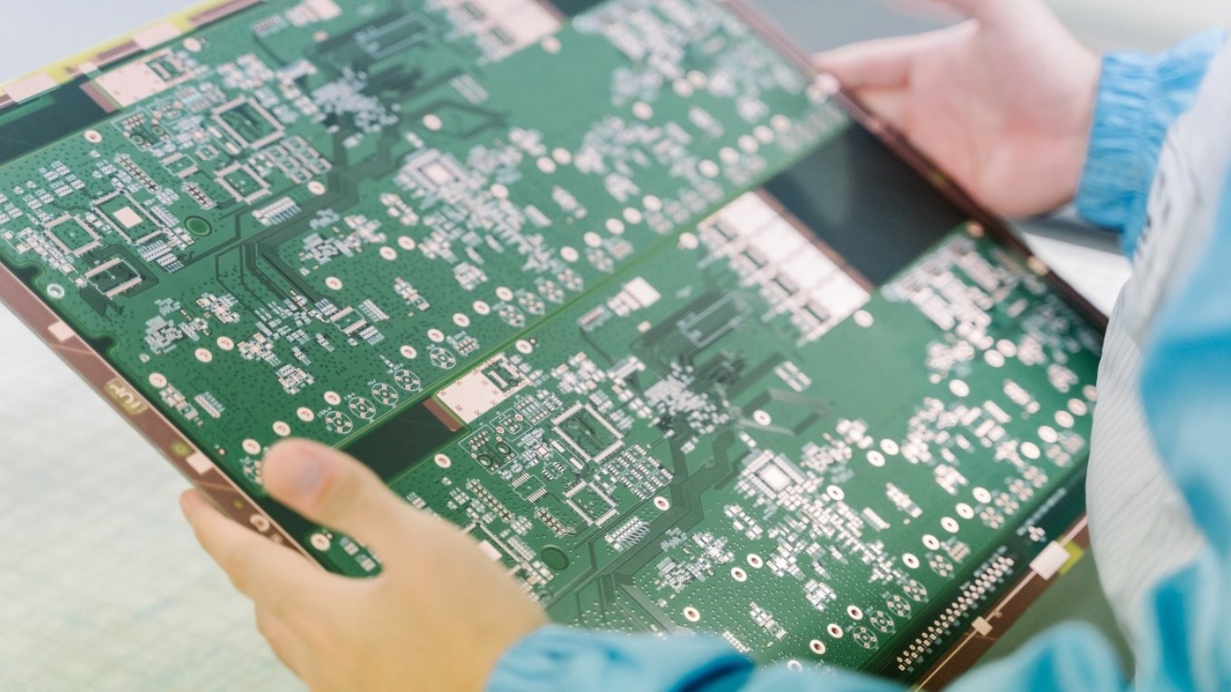
Rule 5: Copy the Required Circuit Board Multiple Times to Another Larger Circuit Board for PCB Imposition.
Choosing the size that best fits the equipment used by the manufacturer will help reduce prototyping and manufacturing costs. First, do the board layout on the panel, contact the board manufacturer to get their preferred size specifications for each panel, then revise your design specifications and try to repeat your design multiple times within those panel sizes.
Rule 6: Integrate Component Values.
The bill of materials can be simplified and costs reduced by integrating within a smaller range of standard values. It will be easier for you to make the right inventory management decisions from a longer-term perspective if you have a range of PCB products based on the value of your preferred components.
Rule 7: Perform Design Rule Checking (DRC) Whenever Possible.
Although it takes only a short time to run the DRC function on the PCB software, in a more complex design environment, it can save a lot of time as long as it is always checked during the design process. This is a good habit worth maintaining.
Rule 8: Make Flexible Use of Screen Printing.
Screen printing can be used to mark various useful information for future use by the board manufacturer, service or test engineer, installer or equipment debugger. Not only clear function and test point labels but also the orientation of components and connectors as much as possible, even if these annotations are printed on the lower surface of the components used on the board (after the board is assembled) On the upper and lower surfaces of the board Full application of screen printing technology can reduce repetitive work and simplify the production process.
Rule 9: Decoupling Capacitors Must Be Chosen.
Don't try to optimize your design by avoiding decoupling power lines and based on limiting values in component datasheets. Capacitors are cheap and durable. You can spend as much time assembling the capacitors as you want. In the meantime, follow rule 6 and use standard value ranges to keep your inventory tidy.
Rule 10: Generate Pcb Manufacturing Parameters and Verify Before Committing to Production.
While most board manufacturers are happy to download it directly and verify it for you, it's best to export the Gerber file yourself and check with a free viewer that it's as expected to avoid misunderstandings. By doing it yourself, you can even spot inadvertent errors and avoid costly production done to the wrong parameters.
The above introduces some rules when designing PCB boards. If you want to order PCB boards, please contact us.
Singo is a professional custom PCB board manufacturer. The company is mainly engaged in PCB assembly and OEM/ODM electronic manufacturing services. Products include household appliances, digital products, industrial controls, medical equipment, etc. After years of hard work, we have established long-term cooperative relationships with some internationally renowned companies. Some of our products are often required to operate in harsh environments where quality and reliability are paramount. With many years of experience, we have won a good reputation from customers in the field of electronic production with reasonable prices, abundant resources and on-time delivery.

