
Key Tips for Reliable Rigid-Flex PCB Design
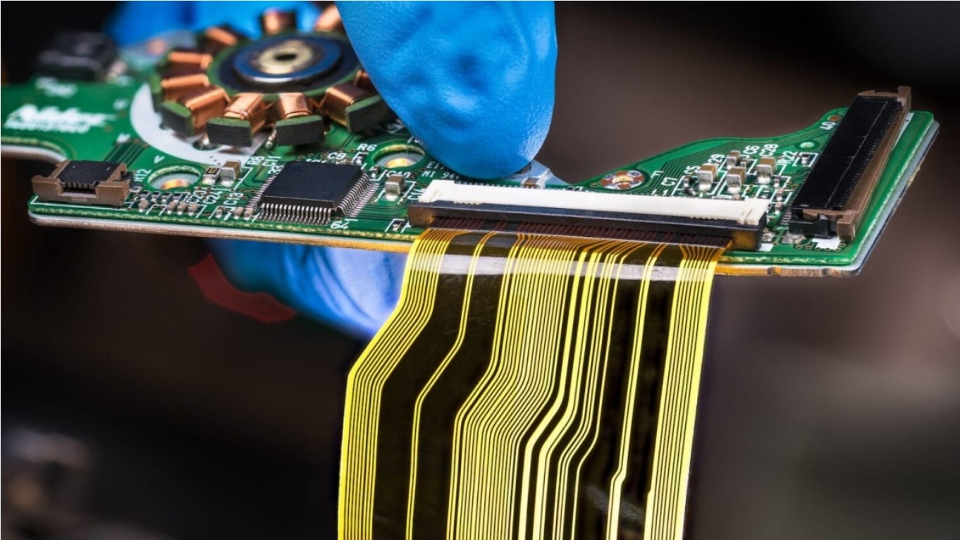
A rigid-flex PCB design combines the best of both worlds - elements of a standard "rigid" (usually FR-4) PCB with a flexible PCB on a single board. These boards mainly consist of two or more rigid areas connected by flexible polyimide strips and copper-clad substrates. Board manufacturers take a rigid board and then add vias to connect it to a flexible polyimide board.
Due to the complexity of the rigid-flex board, its design involves a lot of content. When you apply the design tips and methods we'll discuss, you'll be able to design rigid-flex boards that are reliable and can withstand hundreds of flex cycles without failure.
Rigid-Flex PCB Design Fundamentals
Rigid-flex PCB design involves a lot. First, consider your application and the strengths and weaknesses mentioned earlier. Once you've determined that a rigid-flex PCB design is a way to go, consider the expected environment for your board. Is the plate for dynamic bending or steady bending and what is the bend radius?
Dynamic bending rigid-flex panels are used in environments that are constantly subjected to stress and bending. In this case, use no more than two layers and ensure that the bend radius is at least 100 times the thickness of the flexible material. Once bent or bent, a stable bend means staying in that position. In this case, make sure that the flex substrate thickness is about one-tenth of the bend radius.
Visualize your design in 3D as it will function. Rigid-flex designs are usually placed inside the enclosure. Consider the mechanical forces and stresses the boards may be exposed to, and make sure the boards inside the enclosure are designed to handle them.
Hole, Routing, and Fill Plane Guidelines for Rigid-Flex PCB Design
When designing rigid-flex boards, the most sensitive area is bending. Therefore, avoid placing pads, holes, and vias in these curved areas. The area near the bend line can be mechanically stressed, tearing or damaging the plated hole structure adjacent to it. Place pads and vias on flexible areas that won't bend, or preferably on rigid, hard parts of the PCB.
If you're placing plated holes or vias on the flex, make sure to use anchors to reinforce them, and teardrops to attach any traces. Keep the holes around 10 mils with at least one 10 mil annular ring around them. This larger size allows for easier fixing and prevents peeling during buckling. In general, avoid placing holes, vias, or pads in flexible areas and place as many as possible in rigid areas. Try to keep them at least 15m away from the edge of the stack, as the edges of the board can be more unstable.
Rigid-Flex Board Routing
Regarding your traces and routing, keep your traces straight, vertical lines. If your board is bent or folded along a horizontal line, have your traces run vertically. Ideally, traces should go in one direction, but in cases where a change of direction must be made, the traces should be bent instead of at 45 or 90-degree angles. This will remove high-stress areas on the board. Use narrower traces evenly spaced across flex areas to reduce areas of high stress. Adding dummy traces or even redundant traces can help increase the mechanical robustness of the flex area and prevent traces from completely disrupting the signal path. If you have traces on the top and bottom of the flex section, alternate them so that the bottom trace has no top trace directly above it,
For your power, signal, and ground planes, if you put a solid layer of copper on a typical plane, you end up putting a lot of stress on your board and reducing its flexibility. Instead, use a shaded polygonal pattern for the plane. Also, try to minimize the trace width on the fill, but be aware that cross-hatching is not very good for high-speed signal integrity.
Design Standards for Rigid-Flex Boards
There are many standards for rigid-flex boards that are worth referring to. For example, IPC 2223 specifies overlay construction, bonded flex core, air gap, strain relief fillets, and prebaking requirements for circuit boards. Additionally, it includes hints for locating plated vias or holes near the rigid-to-flex transition region. This area is unique in that the polyimide cover that encapsulates the flexible areas must overlap the rigid areas by a small distance to ensure that they are encapsulated by the rigid areas of the lamination process. Overlays are attached to flexible surfaces using adhesives made from acrylic or epoxy resins. If vias are drilled through adhesive, they may be stressed by expansion or contraction of the adhesive due to the high coefficient of thermal expansion, especially during reflow temperatures.
The above briefly introduces the key skills of rigid-flex PCB design. If you want to customize the PCB board, please contact us.
Singo is a professional custom PCB board manufacturer. We offer full-service PCB assembly and fabrication, so you can have our team on hand throughout the conceptualization phase and successful product launch. Our top priority is to deliver high standards of work and fast turnaround times in everything we do for you. With advanced equipment and skilled engineers, we provide various electronic manufacturing services, and can complete short-term production of up to 10,000 units at a time.
