
How Multilayer PCBs are Made?
When looking for a printed circuit board, you will come across a variety of options for different applications. The most popular examples are conventional rigid PCB rigid-flex PCB, and double-sided multilayer PCB.
Your choices must be carefully checked before making them. More importantly, you should know how to integrate the board with the elements of the application. While there is no final solution for everyone to follow, here is a brief overview of how most manufacturers implement multilayer PCBs.
What is a multilayer PCB?
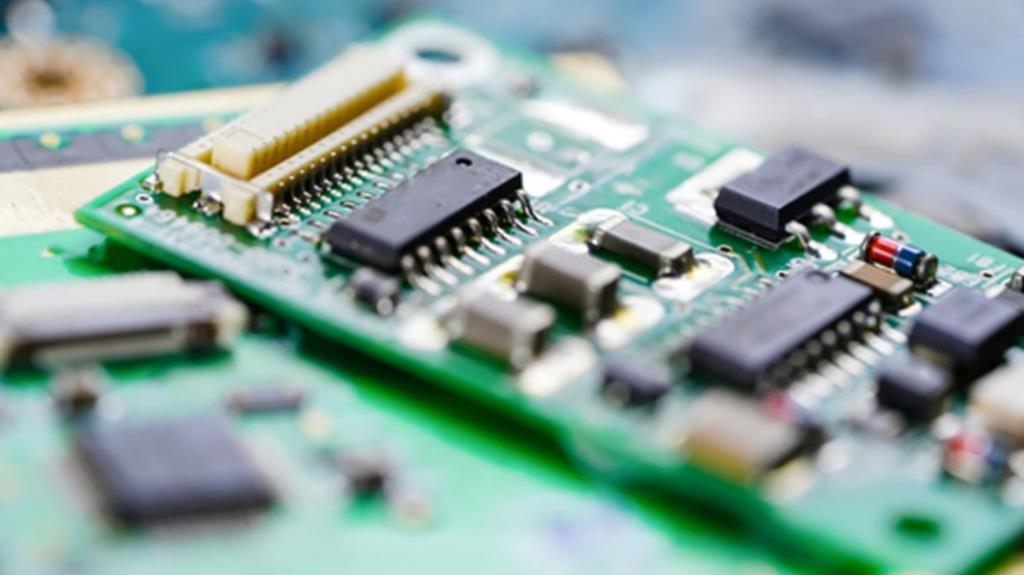
Since rigid circuits have some application requirements, different PCB designs are stacked into a single component. Multilayer PCBs , as the name suggests, is made of two, three, or more circuit boards. Some manufacturers can assemble more than 30 different circuit layers on multiple boards. The PCB has a rigid core, usually made of FR4 and copper. The core is then surrounded with copper foil and PrePeg fiberglass to form a laminate assembly. The process of making a multilayer printed circuit board varies from manufacturer to manufacturer, depending on the board they want to make. A typical four-layer multilayer PCB will include the following sections:
a) FR4 fiberglass laminate
This is the heart of the PCB. Because it provides support for the entire board, this core must be rigid and handled for traces. The core is also slightly thicker than the other layers added to the design.
b) Copper
Immediately after the rigid core is two copper layers, which are designed on either side of the core. Copper separates the core from the B-grade PrePeg glass fibers that make up the next immediate layer.
c) B-Stage PrePeg glass fiber
PrePeg fiberglass simply refers to fiberglass that is still soft and requires heat to harden. Grade B PrePeg fiberglass acts as the glue to attach the inner FR4 core to the copper foil.
This layer consists of thin, loose copper sheets and is the outermost layer in the assembly. The copper foil is sandwiched with the PrePeg and core and placed into the PCB lamination process.
e) Other elements
Multilayer PCBs can be single-sided or double-sided. Double-sided boards are more popular and have interconnected copper patterns on the front and back of the board. The design also features conductive plated drill holes (through holes) that connect one side of the board to the other.
Front-end engineering
This is the first step in making the PCB. At this stage, the manufacturer will check the PCB design to start preparing for production. There are different approaches to this process, but it basically entails developing step-by-step instructions for building a PCB. All designs are reviewed and planners also create "process cards" (travelers) that will move with the PCB throughout the design process. CAM engineers will also conduct a thorough design review and then convert all files to the data format required for manufacturing.
Front-end engineering is more of a planning stage where planners review all requirements and information put forward for PCB production. This includes purchase order details, manufacturing drawings, special instructions, quantities and deadlines, and materials. The CAM engineer is tasked with conducting an in-depth data review and identifying the tools needed to achieve the final product. Engineers typically follow a detailed checklist that includes:
Data cleaning - data needs to be loaded into CAM software to perform data cleaning and editings, such as assigning names and layer alignment.
Drill data validation - this ensures that the hole size counts in the data file match those in manufacturing. It also checks for special wiring, cutouts, and plating requirements.
PCB editing - here, engineers run DRC (Design Rule Check) to preview image files and make useful adjustments. It may include resizing drill holes, editing layers, adding BAC marks, and adding etch compensation.
Panelization - based on a perfect fit, boards are laid out on a production panel using frames, labels, and tools.
Output - this is the final step in front-end fabrication and involves generating different outputs, including drill file AOI (Automated Optical Inspection) path files and image files.
The process of making a multilayer PCB
There are several factors that go into producing high-quality multilayer PCBs. The process involves specific steps required to ensure that each aspect is covered. Due to the different types of multilayer boards, the manufacturing process may vary depending on the unique design you want to achieve. In addition to front-end planning, general procedures include:
Photo drawing - converts photo data and converts it to image pixels.
Imaging and DES (Develop, Etch, Strip) - apply the master image to the PCB.
Automated optical inspection - inspects the number of layers in multilayer PCBs prior to lamination.
Oxidation treatment and lamination - chemical treatment applied to inner layers of PCBs. Lamination bonds different layers of copper and fiberglass together.
Drilling and electroless copper plating - this process creates the required drilled holes and trenches on the PCB. They are then covered with copper deposits.
Electrical testing, fabrication, micro sectioning, and final inspection
Manufacturers may also include other processes to achieve unique designs and specifications. Each step has a unique process that can be customized according to production requirements. Manufacturers can also use different technologies at different stages. For example, some draw on film during the photo drawing process, while others use a special LDI (Laser Direct Imaging). Inspection is also key for any multilayer PCB. They help ensure that the board functions properly and meets customer specifications.
In conclusion
Making a multilayer PCB on paper is a lengthy process. Front-end manufacturing usually takes the longest and manufacturers to use this stage to ensure all requirements, tools, and dimensions are in order. In addition, several tests were performed to troubleshoot and identify any errors in the design. If you are in the multi-layer PCB market, it is recommended to choose an experienced and high-quality circuit board manufacturer to ensure a quality product.
Singo is a professional custom PCB board manufacturer. Our manufacturing facilities include a clean room and advanced high-speed SMT line (Yamaha), a fully automatic printing press, lead-free wave soldering, and a fully automatic assembly line. Our die attaches accuracy can reach ±0.03mm on IC parts. This means we can handle almost all types of ICs such as SO, SOP, SOJ, TSOP, TSSOP, QFP, GA, and U-BGA. We not only have strong OEM manufacturing capabilities and engineering support, but also have excellent experience in R&D, manufacturing, and maintenance testing. If you want to customize the PCB board, welcome to contact us.
